Why should I need to resize a polygon? Most of the multi-layer PCB’s I made had a ground or power plane inside the PCB. In Altium it is possible to implement an internal plane but most designers I know (me as well) don’t like that approach as the copper does reach till the outside of the PCB shape. In most cases I use a polygon connected to ground as internal plane. This polygon is a scaled version of the board shape. To do this Altium Designer should provide the functionality to scale the polygon by a value or percentage. However, Altium does not provide this scaling functionality that’s why I wanted to share my tiny workaround to create the scaled version of the polygon.
(* Press (CTRL+h) and click on the wire to select the whole connection)
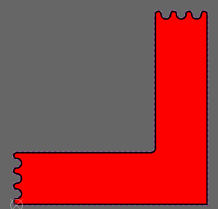
Step 1
- Create the pcb border/shape using a mechanical layer or keep-out layer. For explanation purpose I created an weird example PCB shape.
- Select the board shape (*), Mine was on mechanical layer 1. To create a board shape in Altium press [Design/Board Shape/Define from selected objects] while selecting the objects.
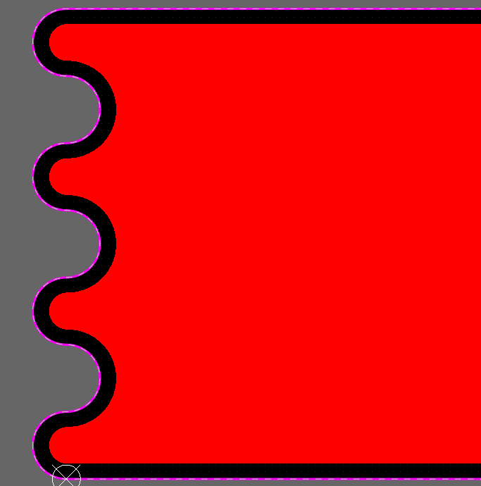
Step 2
- Copy the board shape ( mechanical 1) next to the the PCB.
- Select the copy of the board shape and convert the layer from mechanical 1 to top or bottom layer. It is important that it is a copper layer otherwise it would not work.
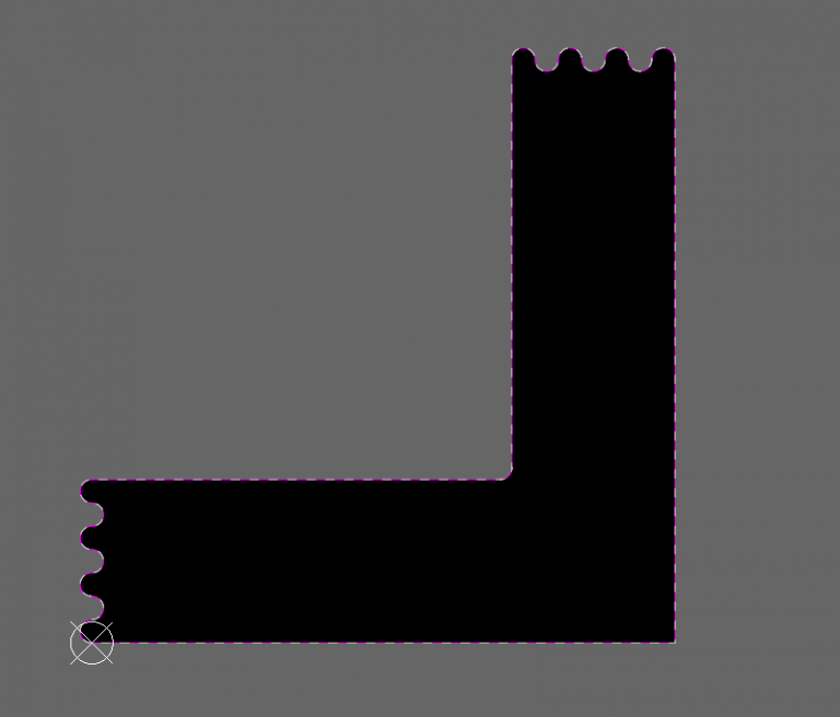
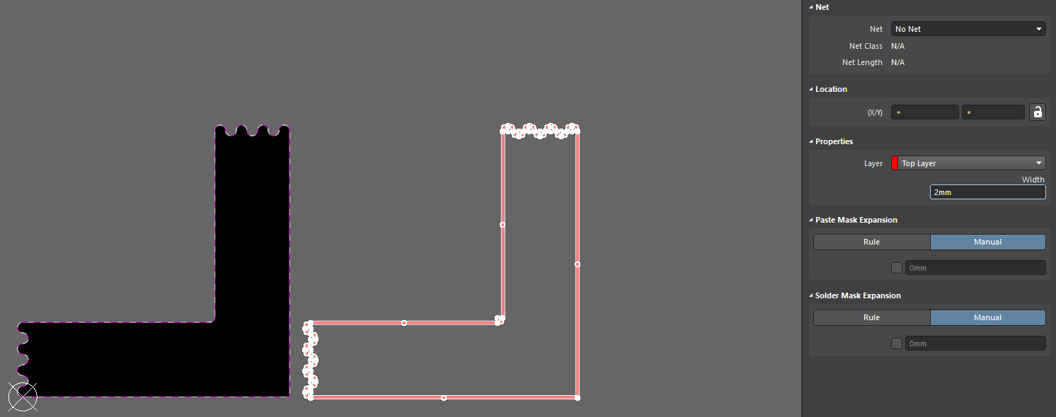
Step 3
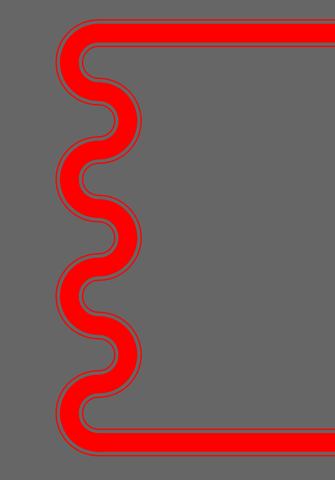
- Change the line width for example toward to 2 mm. This will set the scale factor of the polygon. Thicker lines (3mm, 4mm …) will create a smaller polygon inside this shape.
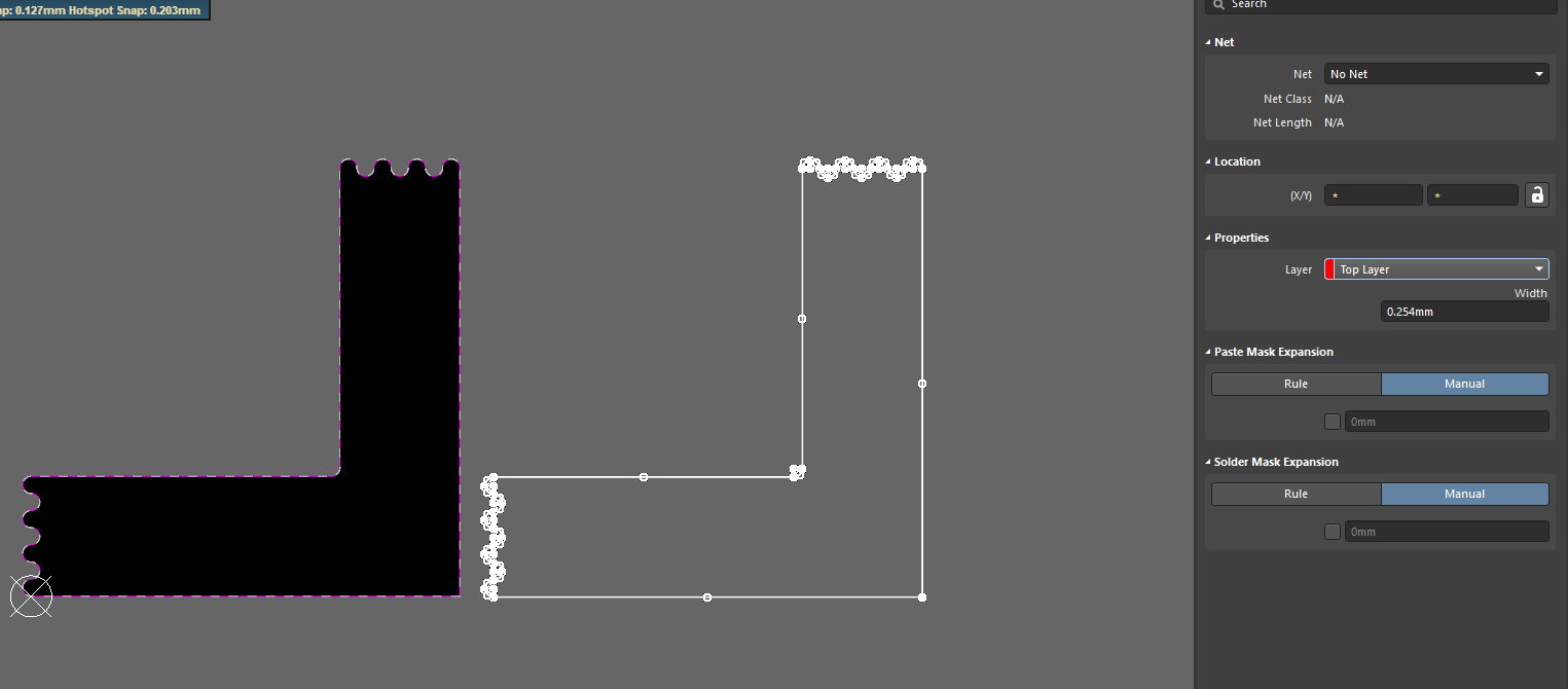
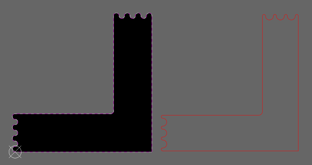
Step 4
- Outline this thicker version of the board shape. Select it (*) and press [Tools/Outline]. The result will look like this figure.
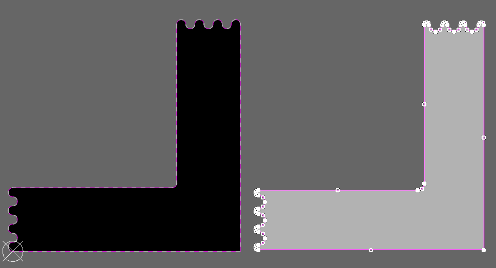
Step 5
- Select the thick line ( * ) as well as the outer version of the thin lines (*) an delete them. To create the scaled polygon only the inner lines are needed.
Step 6
- Select these lines and press [Tools/Convert/Create Polygon from Selected Primitives]. The result is a polygon. You can change the layer of this polygon, as well as the net connection or if it is solid or hatched.
Step 7
Copy this polygon back to the pcb board. You can see that it is a scaled version of the board shape. Resize it by using the same process as explained while changing the line width.